news
Georgia Tech President Cabrera Pays Visit to Khan Lab
Primary tabs
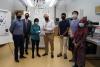
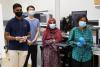
Georgia Tech President Ángel Cabrera recently paid a visit to the Khan Lab, located in the Pettit Microelectronics Building, to learn more about the field of ferroelectricity and negative capacitance and its applications in microelectronics. Douglas M. Blough, the interim Steve W. Chaddick School Chair in the School of Electrical and Computer Engineering (ECE), also took part in the visit.
The Khan Lab is led by Asif Khan, who is an ECE assistant professor and a recent recipient of a DARPA Young Faculty Award, an NSF CAREER Award, and an Intel Rising Star Award. He and his team of six Ph.D. students and two engineers research microelectronic devices to address the challenges faced by the semiconductor technology due to the end of transistor miniaturization. His group focuses on all aspects of ferroelectricity, ranging from materials physics, growth, and electron microscopy to micro-/nano-fabrication of ferroelectronic devices. This includes ferroelectric circuits and systems for artificial intelligence, machine learning, and data-centric applications.
During the visit with Cabrera on August 18, Khan explained the importance of semiconductor electronics in modern times.
“Transistors are the most abundant, man-made artifact in history; more than ten sextillion (1022) transistors have been manufactured since the 1960s,” Khan said. “And they are the basis for the future that technology holds for us, from artificial intelligence, machine learning driven applications, autonomous transportation to space exploration, medicine, and health care.”
Khan also gave an overview of current challenges in microelectronics. “Cloud infrastructure is estimated to account for 1 to 5 percent of worldwide energy consumption and has a significant carbon footprint equivalent to that of mid-sized countries like the Netherlands and Malaysia. Environmental impacts of microelectronics may skyrocket in the next 10 to 15 years with the massive proliferation of information technologies.”
Khan and his team are investigating innovative approaches to curb energy usage in electronics. They gave an overview of the concept of negative capacitance, a phenomenon in ferroelectric materials that can reduce the power dissipation in transistors below the ‘fundamental’ thermodynamic limit. Negative capacitance is an area of interest in multiple fields, including materials science, condensed matter physics, and electrical engineering.
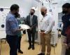
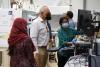
Nujhat Tasneem, a fifth year Ph.D. student, showed a ferroelectric transistor chip fabricated at the Institute of Electronics and Nanotechnology (IEN), an interdisciplinary research institute at Georgia Tech. Besides its negative capacitance properties, FEFETs are also an emerging candidate in the embedded memory space for artificial intelligence applications. Tasneem's work involves characterizing the performance of FEFETs as a memory device. Some of her characterization experiments were also shown to Cabrera. The president’s visit also showcased a state-of-the-art 300 mm ferroelectric wafer that was manufactured at a semiconductor company.
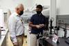
Following Tasneem’s presentation, Prasanna Ravindran, a third year Ph.D. student in the Khan Lab, in collaboration with IEN, demonstrated the use of Microsoft Hololens for remote assistance and effective collaboration for cleanroom activities. The lab started using the technology during the pandemic in order to have discussions with collaborators who were unable to travel, as well as among lab members for remote assistance and for questions about experimental setups and metrology. Khan alluded to the possibilities of using Hololens for many kinds of outreach and general awareness activities, including tours of labs and IEN cleanrooms for K-12 students. Afterwards, Ravindran gave an overview of his cryogenic measurement setup which can measure devices down to 4 K.
Cabrera shared stories of his personal journey, including his diverse professional training in telecommunications engineering and cognitive psychology, and his different leadership roles spanning two different continents. He also mentioned the changing landscape of the metro Atlanta area, especially with the recent arrival of a couple of big-tech companies. Blough described the important role that the School of Electrical and Computer Engineering is playing on the national stage in the areas of semiconductors and nanotechnology.
The visit concluded with an inspiring note from Cabrera to the students and the attendees: “It is always important to remember the impact of your work on society. During the course of a Ph.D., while you are laser-focused on a specific problem, it is easy to lose sight of the big picture,” he said. “In your case, you are addressing a grand challenge that may in some shape or form impact all of us and the ones who will come after us.”
Photo credits: Ashlee Gardner
Media
Summary
Georgia Tech President Ángel Cabrera recently paid a visit to the Khan Lab, located in the Pettit Microelectronics Building, to learn more about the field of ferroelectricity and negative capacitance and its applications in microelectronics.
Status
- Workflow status: Published
- Created by: Jackie Nemeth
- Created: 09/08/2021
- Modified By: Jackie Nemeth
- Modified: 09/08/2021
Categories
Keywords
- Georgia Tech
- School of Electrical and Computer Engineering
- Khan Lab
- Asif Khan
- Ángel Cabrera
- Douglas Blough
- ferroelectricity
- negative capacitance
- microelectronics
- Prasanna Ravindran
- Chinsung Park
- Nashrah Afroze
- Nujhat Tasneem
- Semiconductors
- transistor miniaturization
- Materials Physics
- electron microscopy
- microfabrication
- nano fabrication
- artificial intelligence
- machine learning
- data-centric applications
- cloud infrastructure
- information technology
- Institute of Electronics and Nanotechnology
- FEFETs
- embedded memory
- cleanroom
- cryogenics
- cryogenic measurements
User Data