news
Room-temperature Bonded Interface Improves Cooling of Gallium Nitride Devices
Primary tabs
A room-temperature bonding technique for integrating wide bandgap materials such as gallium nitride (GaN) with thermally conducting materials such as diamond could boost the cooling effect on GaN devices and facilitate better performance through higher power levels, longer device lifetime, improved reliability, and reduced manufacturing costs. The technique could have applications for wireless transmitters, radars, satellite equipment, and other high-power and high-frequency electronic devices.
The technique, called surface-activated bonding, uses an ion source in a high-vacuum environment to first clean the surfaces of the GaN and diamond, which activates the surfaces by creating dangling bonds. Introducing small amounts of silicon into the ion beams facilitates forming strong atomic bonds at room temperature, allowing the direct bonding of the GaN and single-crystal diamond to fabricate high-electron-mobility transistors (HEMTs).
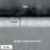
The resulting interface layer from GaN to single-crystal diamond is just four nanometers thick, allowing heat dissipation up to two times more efficient than in the state-of-the-art GaN-on-diamond HEMTs by eliminating the low-quality diamond left over from nanocrystalline diamond growth. Diamond is currently integrated with GaN using crystalline growth techniques that produce a thicker interface layer and low-quality nanocrystalline diamond near the interface. Additionally, the new process can be done at room temperature using surface-activated bonding techniques, reducing the thermal stress applied to the devices.
“This technique allows us to place high thermal conductivity materials much closer to the active device regions in gallium nitride,” said Samuel Graham, the Eugene C. Gwaltney Jr. School Chair and professor in Georgia Tech’s George W. Woodruff School of Mechanical Engineering. “The performance allows us to maximize the performance for gallium nitride on diamond systems. This will allow engineers to custom design future semiconductors for better multifunctional operation.”
The research, conducted in collaboration with scientists from Meisei University and Waseda University in Japan, was reported February 19 in the journal ACS Applied Materials and Interfaces. The work was supported by a multidisciplinary university research initiative (MURI) project from the U.S. Office of Naval Research (ONR).
For high-power electronic applications using materials such as GaN in miniaturized devices, heat dissipation can be a limiting factor in power densities imposed on the devices. By adding a layer of diamond, which conducts heat five times better than copper, engineers have tried to spread and dissipate the thermal energy.
However, when diamond films are grown on GaN, they must be seeded with nanocrystalline particles around 30 nanometers in diameter, and this layer of nanocrystalline diamond has low thermal conductivity – which adds resistance to the flow of heat into the bulk diamond film. In addition, the growth takes place at high temperatures, which can create stress-producing cracks in the resulting transistors.
“In the currently used growth technique, you don’t really reach the high thermal conductivity properties of the microcrystalline diamond layer until you are a few microns away from the interface,” Graham said. “The materials near the interface just don’t have good thermal properties. This bonding technique allows us to start with ultra-high thermal conductivity diamond right at the interface.”
By creating a thinner interface, the surface-activated bonding technique moves the thermal dissipation closer to the GaN heat source.
“Our bonding technique brings high thermal conductivity single crystal diamond closer to the hotspots in the GaN devices, which has the potential to reshape the way these devices are cooled,” said Zhe Cheng, a recent Georgia Tech Ph.D. graduate who is the paper’s first author. “And because the bonding takes place near room temperature, we can avoid thermal stresses that can damage the devices.”
That reduction in thermal stress can be significant, going from as much as 900 megapascals (MPa) to less than 100 MPa with the room temperature technique. “This low stress bonding allows for thick layers of diamond to be integrated with the GaN and provides a method for diamond integration with other semiconductor materials,” Graham said.
Beyond the GaN and diamond, the technique can be used with other semiconductors, such as gallium oxide, and other thermal conductors, such as silicon carbide. Graham said the technique has broad applications to bond electronic materials where thin interfacial layers are advantageous.
“This new pathway gives us the ability to mix and match materials,” he said. “This can provide us with great electrical properties, but the clear advantage is a vastly superior thermal interface. We believe this will prove to be the best technology available so far for integrating wide bandgap materials with thermally conducting substrates.”
In future work, the researchers plan to study other ion sources and evaluate other materials that could be integrated using the technique.
“We have the ability to choose processing conditions as well as the substrate and semiconductor material to engineer heterogenous substrates for wide bandgap devices,” Graham said. “That allows us to choose the materials and integrate them to maximize electrical, thermal, and mechanical properties.”
In addition to the researchers already mentioned, the paper included co-corresponding author Fengwen Mu from Meisei University and Waseda University in Japan, Luke Yates from Georgia Tech, and Tadatomo Suga from Meisei University.
This research was supported by the U.S. Office of Naval Research (ONR) through MURI Grant No. N00014-18-1-2429. Any findings, conclusions, and recommendations are those of the authors and not necessarily of the Office of Naval Research.
CITATION: Zhe Cheng, Fengwen Mu, Luke Yates, Tadatomo Suga and Samuel Graham, “Interfacial Thermal Conductance across Room-Temperature-Bonded GaN/Diamond Interfaces for GaN-on-Diamond Devices” (ACS Appl. Mater. Interfaces, 2020, 12, 8376?8384). https://doi.org/10.1021/acsami.9b16959
Research News
Georgia Institute of Technology
177 North Avenue
Atlanta, Georgia 30332-0181 USA
Media Relations Contact: John Toon (404-894-6986) (jtoon@gatech.edu).
Media

Summary
A room-temperature bonding technique for integrating wide bandgap materials such as gallium nitride (GaN) with thermally conducting materials such as diamond could boost the cooling effect on GaN devices and facilitate better performance through higher power levels, longer device lifetime, improved reliability, and reduced manufacturing costs. The technique could have applications for wireless transmitters, radars, satellite equipment, and other high-power and high-frequency electronic devices.
Status
- Workflow status: Published
- Created by: John Toon
- Created: 03/16/2020
- Modified By: John Toon
- Modified: 03/16/2020
Keywords
User Data