news
Magnetic Testing Process Helps Ensure Reliability of Microelectronic Devices
Primary tabs
Taking advantage of the force generated by magnetic repulsion, researchers have developed a new technique for measuring the adhesion strength between thin films of materials used in microelectronic devices, photovoltaic cells and microelectromechanical systems (MEMS).
The fixtureless and noncontact technique, known as the magnetically actuated peel test (MAPT), could help ensure the long-term reliability of electronic devices, and assist designers in improving resistance to thermal and mechanical stresses.
“Devices are becoming smaller and smaller, and we are driving them to higher and higher performance,” said Suresh Sitaraman, a professor in the George W. Woodruff School of Mechanical Engineering at the Georgia Institute of Technology. “This technique would help manufacturers know that their products will meet reliability requirements, and provide designers with the information they need to choose the right materials to meet future design specifications over the lifetimes of devices.”
The research has been supported by the National Science Foundation, and was reported in the March 30, 2012 issue of the journal Thin Solid Films.
Modern microelectronic chips are fabricated from layers of different materials – insulators and conductors – applied on top of one another. Thermal stress can be created when heat generated during the operation of the devices causes the materials of adjacent layers to expand, which occurs at different rates in different materials. The stress can cause the layers to separate, a process known as delamination or de-bonding, which is a major cause of microelectronics failure.
“We need to find out if these layers will separate over time as they are used and subjected to thermal and other stresses,” Sitaraman explained. “These systems are used in a wide range of applications from cell phones and computers to automobiles, aircraft and medical equipment. They must be reliable over the course of their expected lifetimes.”
Sitaraman and doctoral student Gregory Ostrowicki have used their technique to measure the adhesion strength between layers of copper conductor and silicon dioxide insulator. They also plan to use it to study fatigue cycling failure, which occurs over time as the interface between layers is repeatedly placed under stress. The technique may also be used to study adhesion between layers in photovoltaic systems and in MEMS devices.
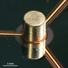
The Georgia Tech researchers first used standard microelectronic fabrication techniques to grow layers of thin films that they want to evaluate on a silicon wafer. At the center of each sample, they bonded a tiny permanent magnet made of nickel-plated neodymium (NdFeB), connected to three ribbons of thin-film copper grown atop silicon dioxide on a silicon wafer.
The sample was then placed into a test station that consists of an electromagnet below the sample and an optical profiler above it. Voltage supplied to the electromagnet was increased over time, creating a repulsive force between the like magnetic poles. Pulled upward by the repulsive force on the permanent magnet, the copper ribbons stretched until they finally delaminated.
With data from the optical profiler and knowledge of the magnetic field strength, the researchers can provide an accurate measure of the force required to delaminate the sample. The magnetic actuation has the advantage of providing easily controlled force consistently perpendicular to the silicon wafer.
Because many samples can be made at the same time on the same wafer, the technique can be used to generate a large volume of adhesion data in a timely fashion.
But device failure often occurs gradually over time as the layers are subjected to the stresses of repeated heating and cooling cycles. To study this fatigue failure, Sitaraman and Ostrowicki plan to cycle the electromagnet’s voltage on and off.
“A lot of times, layers do not delaminate in one shot,” Sitaraman said. “We can test the interface over hundreds or thousands of cycles to see how long it will take to delaminate and for that delamination damage to grow.”
The test station is small enough to fit into an environmental chamber, allowing the researchers to evaluate the effects of high temperature and/or high humidity on the strength of the thin film adhesion. This is particularly useful for electronics intended for harsh conditions, such as automobile engine control systems or aircraft avionics, Sitaraman said.
“We can see how the adhesion strength changes or the interfacial fracture toughness varies with temperature and humidity for a wide range of materials,” he explained.
So far, Sitaraman and Ostrowicki have studied thin film layers about one micron in thickness, but say their technique will work on layers that are of sub-micron thickness. Because their test layers are made using standard microelectronic fabrication techniques in Georgia Tech’s clean rooms, Sitaraman believes they accurately represent the conditions of real devices.
“To get meaningful results, you need to have representative processes and representative materials and representative interfaces so that what is measured is what a real application would face,” he said. “We mimic the processing conditions and techniques that are used in actual microelectronics fabrication.”
As device sizes continue to decline, Sitaraman says the interfacial issues will grow more important.
“As we continue to scale down the transistor sizes in microelectronics, the layers will get thinner and thinner,” he said. “Getting to the nitty-gritty detail of adhesion strength for these layers is where the challenge is. This technique opens up new avenues.”
Research News & Publications Office
Georgia Institute of Technology
75 Fifth Street, N.W., Suite 314
Atlanta, Georgia 30308 USA
Media Relations Contacts: John Toon (404-894-6986)(jtoon@gatech.edu) or Abby Robinson (404-894-6986)(abby@innovate.gatech.edu).
Writer: John Toon


Summary
Taking advantage of the force generated by magnetic repulsion, researchers have developed a new technique for measuring the adhesion strength between thin films of materials used in microelectronic devices, photovoltaic cells and microelectromechanical systems (MEMS).
Groups
Status
- Workflow status: Published
- Created by: John Toon
- Created: 04/11/2012
- Modified By: Fletcher Moore
- Modified: 10/07/2016
Categories
Keywords
User Data