news
Large-area Flexible Organic Photodiodes Can Compete With Silicon Devices
Primary tabs
The performance of flexible large-area organic photodiodes has advanced to the point that they can now offer advantages over conventional silicon photodiode technology, particularly for applications such as biomedical imaging and biometric monitoring that require detecting low levels of light across large areas.
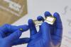
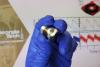
The low-noise, solution-processed, flexible organic devices offer the ability to use arbitrarily shaped, large-area photodiodes to replace complex arrays that would be required with conventional silicon photodiodes, which can be expensive to scale up for large-area applications. The organic devices provide performance comparable to that of rigid silicon photodiodes in the visible light spectrum — except in response time.
“What we have achieved is the first demonstration that these devices, produced from solution at low temperatures, can detect as little as a few hundred thousand photons of visible light every second, similar to the magnitude of light reaching our eye from a single star in a dark sky,” said Canek Fuentes-Hernandez, principal research scientist in the School of Electrical and Computer Engineering at the Georgia Institute of Technology. “The ability to coat these materials onto large-area substrates with arbitrary shapes means that flexible organic photodiodes now offer some clear advantages over state-of-the-art silicon photodiodes in applications requiring response times in the range of tens of microseconds.”
The development and performance of large-area, low-noise organic photodiodes are described in the Nov. 6 issue of the journal Science. The research was supported by multiple organizations, including the Office of Naval Research, the Air Force Office of Scientific Research, and the U.S. Department of Energy’s National Nuclear Security Administration.
Organic electronic devices are based on materials fabricated from carbon-based molecules or polymers instead of conventional inorganic semiconductors such as silicon. The devices can be made using simple solution and inkjet printing techniques instead of the expensive and complex processes involved in the manufacturing of conventional electronics. The technology is now widely used in displays, solar cells, and other devices.
The organic photodiodes use polyethylenimine, an amine-containing polymer surface modifier found to produce air-stable, low work-function electrodes in photovoltaic devices developed in the laboratory of Bernard Kippelen, Joseph M. Pettit Professor at Georgia Tech. The use of polyethylenimine was also shown to produce photovoltaic devices with low levels of dark current — the electrical current that flows through a device even in the dark. This meant the materials could be useful in photodetectors for capturing faint signals of visible light.
“Over the years, the dark current levels were reduced so much that measurement equipment had to be redesigned to detect an electronic noise corresponding to a fluctuation of one electron in one millionth of a second,” Fuentes-Hernandez, the paper’s first author, said. “This work reflects sustained team efforts made in the Kippelen group over more than six years and encompasses part of the Ph.D. work of recent graduates Talha Kahn and Wen-Fang Chou. These collective efforts produced the scientific insights needed to demonstrate organic photodiodes with this level of performance.”
One application for the new devices is in pulse oximeters now placed on fingers to measure heart rate and blood oxygen levels. Organic photodiodes may allow multiple devices to be placed on the body and operate with 10 times less light than conventional devices. This could enable wearable health monitors to produce improved physiological information and continuous monitoring without frequent battery changes. Other potential applications include human-computer interfaces such as touchless gesture recognition and controls.
A future application is detection of ionizing radiation by scintillation — a flash of light emitted by a phosphor when struck by a high energy particle. Lowering the level of light that can be detected would improve the sensitivity of the device, allowing it to detect lower levels of radiation. Detecting radiation emitted from vehicles or cargo containers requires a large detector area, which would be easier to make from organic photodiodes than from arrays of silicon photodiodes.
Organic photodiodes could have similar advantages in X-ray equipment, where doctors want to use the smallest level of radiation possible to minimize the dose delivered to the patient. Here again, sensitivity, large area, and flexible form factor should give organic photodiodes an advantage over silicon-based arrays.
“We are working on improving the response time of the photodetector because producing fast photodetectors would enable many additional important applications,” Fuentes-Hernandez said. “There’s a real need to develop photodetector technologies that are more scalable, and one of the motivations of this work is to advance organic technology that we know is cost effective for scaling.”
The organic photodiodes can show electronic noise current values in the tens of femtoampere range and noise equivalent power values of a couple of hundreds of femtowatt. Key performance factors of the organic photodiodes compare well with silicon except in the area of response time, where researchers are working on a hundred-fold improvement to enable future applications.
“Because we use materials that are processed from inks using printing techniques, they are not as ordered as crystalline materials,” Kippelen said. “As a result, the carrier mobility and the velocity of the carriers that can move through these materials are lower, so you can’t get the same fast signals you get with silicon. But for many applications you don’t need picosecond or nanosecond response time.”
For Kippelen, the photodiode work shows the results of a 25-year effort to improve the performance of organic electronic materials. That work, part of Georgia Tech’s Center for Organic Photonics and Electronics, has involved extensive device modeling to understand the basic science, and research to continuously boost performance of the materials.
“Organic thin films absorb light more efficiently than silicon, so the overall thickness you need to absorb that light is very small,” Kippelen said. “Even if you scale their area up, the overall volume of your detector remains small with organics. If you increase the area of a silicon detector, you have a larger volume of materials that at room temperature will generate a lot of electronic noise.”
The photodiodes made in Kippelen’s lab use an active layer just 500 nanometers thick. A gram of the material, roughly the size of a fingertip, could coat the surface of an office desk.
Kippelen hopes the Science paper will help open new doors for organic semiconductors.
“Advances like this will allow us to change the conventional wisdom that switching to organic materials that can lead to scalable devices would mean giving up performance,” he said. “We can’t anticipate all the new applications that could be enabled by this advance.”
In addition to those already mentioned, the research team included Larissa Diniz, Julia Lukens, Felipe A. Larrain, and Victor A. Rodriguez-Toro, all associated with Kippelen’s lab.
This research was supported by the Department of the Navy, Office of Naval Research Awards N00014-15 14-1-0580 and N00014-16-1-2520; through the MURI Center for Advanced Organic Photovoltaics (CAOP); by the Air Force Office of Scientific Research through Award No. FA9550-16-1-0168, the Department of Energy / National Nuclear Security Administration (NNSA) awards DE-NA0002576 through the Consortium for Nonproliferation Enabling Capabilities (CNEC), and award DE-NA0003921 through the Consortium for Enabling Technologies and Innovation. Support also came from the Chilean National Commission for Scientific and Technological Research through the Doctoral Fellowship program ‘‘Becas Chile,’’ Grant 72150387; from the Colombian Administrative Department of Science, Technology, and Innovation through the program Fulbright-Colciencias; from the National Science Foundation through the Research Experiences for Undergraduates program; and from the Brazil Scientific Mobility Program through an Academic Training Opportunities grant.
CITATION: Canek Fuentes-Hernandez, et al., “Large-area low-noise flexible organic photodiodes for detecting faint visible light.” (Science 2020).
Research News
Georgia Institute of Technology
177 North Avenue
Atlanta, Georgia 30332-0181 USA
Media Relations Contact: John Toon (404-894-6986) (jtoon@gatech.edu)
Writer: John Toon
Media

Summary
The performance of flexible large-area organic photodiodes has advanced to the point that they can now offer advantages over conventional silicon photodiode technology, particularly for applications such as biomedical imaging and biometric monitoring that require detecting low levels of light across large areas.
Groups
Status
- Workflow status: Published
- Created by: John Toon
- Created: 11/05/2020
- Modified By: John Toon
- Modified: 11/05/2020
Categories
Keywords
User Data