news
Nanostructured Gate Dielectric Boosts Stability of Organic Thin-Film Transistors
Primary tabs
A nanostructured gate dielectric may have addressed the most significant obstacle to expanding the use of organic semiconductors for thin-film transistors. The structure, composed of a fluoropolymer layer followed by a nanolaminate made from two metal oxide materials, serves as gate dielectric and simultaneously protects the organic semiconductor – which had previously been vulnerable to damage from the ambient environment – and enables the transistors to operate with unprecedented stability.
The new structure gives thin-film transistors stability comparable to those made with inorganic materials, allowing them to operate in ambient conditions – even underwater. Organic thin-film transistors can be made inexpensively at low temperature on a variety of flexible substrates using techniques such as inkjet printing, potentially opening new applications that take advantage of simple, additive fabrication processes.
“We have now proven a geometry that yields lifetime performance that for the first time establish that organic circuits can be as stable as devices produced with conventional inorganic technologies,” said Bernard Kippelen, the Joseph M. Pettit professor in Georgia Tech’s School of Electrical and Computer Engineering (ECE) and director of Georgia Tech’s Center for Organic Photonics and Electronics (COPE). “This could be the tipping point for organic thin-film transistors, addressing long-standing concerns about the stability of organic-based printable devices.”
The research was reported January 12 in the journal Science Advances. The research is the culmination of 15 years of development within COPE and was supported by sponsors including the Office of Naval Research, the Air Force Office of Scientific Research, and the National Nuclear Security Administration.
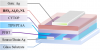
Transistors comprise three electrodes. The source and drain electrodes pass current to create the “on” state, but only when a voltage is applied to the gate electrode, which is separated from the organic semiconductor material by a thin dielectric layer. A unique aspect of the architecture developed at Georgia Tech is that this dielectric layer uses two components, a fluoropolymer and a metal-oxide layer.
“When we first developed this architecture, this metal oxide layer was aluminum oxide, which is susceptible to damage from humidity,” said Canek Fuentes-Hernandez, a senior research scientist and coauthor of the paper. “Working in collaboration with Georgia Tech Professor Samuel Graham, we developed complex nanolaminate barriers which could be produced at temperatures below 110 degrees Celsius and that when used as gate dielectric, enabled transistors to sustain being immersed in water near its boiling point.”
The new Georgia Tech architecture uses alternating layers of aluminum oxide and hafnium oxide – five layers of one, then five layers of the other, repeated 30 times atop the fluoropolymer – to make the dielectric. The oxide layers are produced with atomic layer deposition (ALD). The nanolaminate, which ends up being about 50 nanometers thick, is virtually immune to the effects of humidity.
“While we knew this architecture yielded good barrier properties, we were blown away by how stably transistors operated with the new architecture,” said Fuentes-Hernandez. “The performance of these transistors remained virtually unchanged even when we operated them for hundreds of hours and at elevated temperatures of 75 degrees Celsius. This was by far the most stable organic-based transistor we had ever fabricated.”
For the laboratory demonstration, the researchers used a glass substrate, but many other flexible materials – including polymers and even paper – could also be used.
In the lab, the researchers used standard ALD growth techniques to produce the nanolaminate. But newer processes referred to as spatial ALD – utilizing multiple heads with nozzles delivering the precursors – could accelerate production and allow the devices to be scaled up in size. “ALD has now reached a level of maturity at which it has become a scalable industrial process, and we think this will allow a new phase in the development of organic thin-film transistors,” Kippelen said.
An obvious application is for the transistors that control pixels in organic light-emitting displays (OLEDs) used in such devices as the iPhone X and Samsung phones. These pixels are now controlled by transistors fabricated with conventional inorganic semiconductors, but with the additional stability provided by the new nanolaminate, they could perhaps be made with printable organic thin-film transistors instead.
Internet of things (IoT) devices could also benefit from fabrication enabled by the new technology, allowing production with inkjet printers and other low-cost printing and coating processes. The nanolaminate technique could also allow development of inexpensive paper-based devices, such as smart tickets, that would use antennas, displays and memory fabricated on paper through low-cost processes.
But the most dramatic applications could be in very large flexible displays that could be rolled up when not in use.
“We will get better image quality, larger size and better resolution,” Kippelen said. “As these screens become larger, the rigid form factor of conventional displays will be a limitation. Low processing temperature carbon-based technology will allow the screen to be rolled up, making it easy to carry around and less susceptible to damage.
For their demonstration, Kippelen’s team – which also includes Xiaojia Jia, Cheng-Yin Wang and Youngrak Park – used a model organic semiconductor. The material has well-known properties, but with carrier mobility values of 1.6 cm2/Vs isn’t the fastest available. As a next step, they researchers would like to test their process on newer organic semiconductors that provide higher charge mobility. They also plan to continue testing the nanolaminate under different bending conditions, across longer time periods, and in other device platforms such as photodetectors.
Though the carbon-based electronics are expanding their device capabilities, traditional materials like silicon have nothing to fear.
“When it comes to high speeds, crystalline materials like silicon or gallium nitride will certainly have a bright and very long future,” said Kippelen. “But for many future printed applications, a combination of the latest organic semiconductor with higher charge mobility and the nanostructured gate dielectric will provide a very powerful device technology.”
This research was supported in part by the Center for Organic Photonics and Electronics at Georgia Tech, by the Department of the Navy, Office of Naval Research Awards N00014-14-1-0580 and N00014-16-1-2520, through the MURI Center for Advanced Photovoltaics (CAOP), by the Air Force Office of Scientific Research through Award No. FA9550-16-1-0168, by the National Nuclear Security Administration Award DE-NA0002576 through the Consortium for Nonproliferation Enabling Technologies (CNEC). Seminal work on the concept of using a bilayer gate dielectric in OFETs was funded in part by Solvay S.A. and described in part in issued patent No. US 9,368,737 B2.
CITATION: Xiaojia Jia, Canek Fuentes-Hernandez, Cheng-Yin Wang, Youngrak Park, Bernard Kippelen, “Stable organic thin-film transistors,” (Science Advances, 2018).
Research News
Georgia Institute of Technology
177 North Avenue
Atlanta, Georgia 30332-0181 USA
Media Relations Contacts: John Toon (404-894-6986) (jtoon@gatech.edu) or Josh Brown (404-385-0500) (josh.brown@comm.gatech.edu)
Writer: John Toon


Summary
A nanostructured gate dielectric developed in the labs of STAMI-COPE Professor Bernard Kippelen may have addressed the most significant obstacle to expanding the use of organic semiconductors for thin-film transistors. The structure, composed of a fluoropolymer layer followed by a nanolaminate made from two metal oxide materials, serves as gate dielectric and simultaneously protects the organic semiconductor – which had previously been vulnerable to damage from the ambient environment – and enables the transistors to operate with unprecedented stability.
For more see the Article in Georgia Tech Research Horizons
Status
- Workflow status: Published
- Created by: Tim Parker
- Created: 08/07/2018
- Modified By: Tim Parker
- Modified: 08/07/2018
User Data