news
What’s New in Packaging @ Georgia Tech? Wafer Fan-Out is a Great Success. What Next?
Primary tabs
Georgia Tech Developing Ultra-thin Glass Panel Embedding (GPE) for a combination of highest I/O density, lowest RC delay, thinnest size and lowest cost
Embedded Wafer-Fan-Out (WFO), as an outgrowth of wafer level packaging with fan-out I/Os, has been a great success. It provided a path for wafer foundries to get into packaging with the most advanced wafer-based materials and tools. It has been applied for analog and digital applications. One of the most recent applications is the Integrated Fanout (InFO) packaging by TSMC for Apple processor and memory to achieve unparalleled bandwidth in a consumer product. This has caused a disruptive change from substrate-based flip-chip packaging, the most dominant packaging technology until then. The primary benefits of this technology are many and include not requiring assembly, and not requiring a substrate with wiring. But its manufacturing processes require reconstitution of diced ICs to be embedded in either molded epoxy or laminates, both limiting the ultimate potential of this technology.
Limitations of WFO
Wafer fanout, however, is limited in achieving its full potential in future generations. Future packages are multi-chip heterogeneous packages with some passive components to form SiPs. Such packages will be large in size. If these embedded packages are applied for high-performance digital applications, requiring logic and HBM chips, they may be even larger. In addition, they need to have ultra-high I/O density between logic and memory with ultra-short interconnect length, and, in addition, require high power and high heat flux dissipation. Current WFO technologies are limited in 7 ways: (1) large die shifts during molding and curing, (2) high warpage, (3) rough surface of molded wafers for precision RDL fabrication, (4) large CTE mismatch between WFO package and the board, affecting reliability, especially for large package sizes, (5) high dimensional instability of molded WFO package for fine lines and vias, requiring large capture pads, (6) coarse through mold or through encapsulant via pitch, and (7) low thermal dissipation due to embedding of ICs into low thermal-conductivity mold compound or laminate substrates.
Georgia Tech’s Inorganic Glass Panel Embedding (GPE) Approach not limited by molding compounds:
Georgia Tech proposes and is developing Ultra-thin Glass Panel Embedding (GPE), as shown in Figure 1, as a pioneering, inorganic approach to embedding with unlimited potential, in performance, thickness, hermeticity, reliability and cost. The GPE approach overcomes all the above 7 limitations as described below. Georgia Tech is developing this technology with its 40 supply-chain industry partners who are supplying the latest and most advanced materials and large area tools. The technology is being developed for a wide array of applications that include: 1) ultra-high bandwidth computing, 2) 5G and millimeter wave communications, 3) sensors for autonomous driving, 4) IoTs, 5) flexible and wearables, 6) low power for computing and high-power for electric cars requiring high-temperature electronics. In GPE, chips are embedded face-up in glass cavities by means of ultra-thin adhesive bonding, followed by dielectric lamination and gap filling, followed by advanced RDL processes that Georgia Tech has been developing to 1 micron line and via.
GPE Building Block Technologies Address the Above 7 Challenges:
GPE building blocks are being developed to address the 7 challenges of WFO as described below.
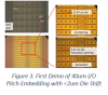
(1) Die shift is dramatically reduced from greater than 25um for WLFO to less than 5um for GPE, by eliminating dimensionally-unstable molding compounds and replacing them with glass that is perfectly CTE-matched to ICs. High-precision cavities are formed at ultra-high throughput in 50-100um thin glass panels by etching, laser ablation or mechanical machining, as shown in Figure 2. The die placement processes into glass cavities were optimized and less than 1-2 um die drifts have been consistently achieved on 150mm panels. This led to the first ever demonstration of the ability to land laser vias on 40um pitch HBM I/O pads on a test chip provided by Global Foundries, as shown in Figure 3.
(2) Warpage: Up to 2-4x reduction in warpage has been demonstrated with GPE, compared to WFO, due to its ability to match the CTE of glass to large ICs, and by eliminating the cure shrinkage of mold encapsulation. Warpage of less than 200um on a 300mm wafer-equivalent area has been shown in GPE panels, compared to >1mm in WFO. This warpage reduction is critical to achieve high-density RDL by lithographic processes.
(3) Surface Roughness: Glass is drawn into sheets, resulting in ultra-smooth surfaces with 1-2nm average roughness. Mold compounds, on the other hand, have a very rough surface after curing due to high filler particle loading, and require expensive grind and polish steps to achieve a smooth surface.
(4) Chip- and Board-Level Reliability: The CTE of glass can be tailored anywhere from 3ppm/C to 11ppm/C, all ready for ultra-thin large panel or roll-to-roll processing to meet chip-level and board-level reliability requirements for large package sizes. WFO is limited to small and medium size packages since mold compounds cannot achieve ultra-low CTE to minimize warpage and die shifts. Low and high CTE glass packages, as large as 20-30mm, and SMT attached to PWBs, have passed 1000s of thermal cycles and more than 20 drops, in previous testing by GT and its partners.
(5) Silicon-like RDL: Glass is an extremely dimensionally-stable material with a Tg of 550C and higher, and does not change in XY dimensions during multi-layer RDL processing. This characteristic of inorganic materials like silicon and glass make them the only base materials on which multilayer RDL can be fabricated with lines and vias of same sizes and scaling to 1-2um dimensions. The GT team has demonstrated the first ever Si BEOL like RDL on panels in the packaging world in 2017, as shown in Figure 4.
(6) Through Vias for 3D Integration: Laminate package through-vias are limited to 300um pitch and through-mold vias by laser processes have been limited to 200um pitch, but ultra-fine pitch through package vias (TPVs) in glass have been demonstrated down to 30um pitch, and can be further scaled due to the availability of high-aspect ratio via formation methods in ultra-thin glass panels.
(7) Thermal: Glass is a poor thermal conductor, but the best thermal conductor in packaging is copper with k values 3-4 times higher than that of silicon. Large copper structures are embedded in glass cavities and connected to the embedded ICs with near-zero thermal resistance interfaces, resulting in significantly better thermal dissipation of GPE packages for higher power-density applications.
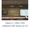
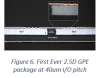
GPE is ultra-thin, using glass layers only 50-70 um thick. The GT team first demonstrated a fully-integrated GPE package with less than 215um total thickness in 2016 as shown in Figure 5. The combination of ultra-low die shifts, ultra-smooth surface and low warpage, and ultra-fine pitch RDL formation on glass led to the first ever demonstration of a 40um I/O pitch 2.5D GPE package, as shown in Figure 6. This breakthrough technology will be presented at IEEE ECTC conference in June 2018 in San Diego, CA.
GPE Applications
Georgia Tech is applying Glass Panel Embedding to a variety of heterogeneous package integration (HPI) applications, including logic-memory integration for high-performance computing, 5G and mm-wave for high-bandwidth wireless, IVRs for power modules, RADAR modules for autonomous driving, and many more.
Digital – Smartphone and HPC:
3D GPE is being applied to logic-memory integration for smartphone applications, with much higher bandwidth and I/O density than WLFO due to the smaller and finer pitch TPVs in glass. In high performance computing, silicon interposers are the primary approach today for logic-memory bandwidth. Although current Silicon interposers are capable of scaling to sub-micron wiring densities, they are ultimately bump limited, due to the limits of solder scaling. They also require additional BGA packages to connect to boards to ensure reliability. GPE is being applied to multi-chip 2.5D interposers to scale not only the RDL, but also the chip-to-package bump interconnects to Back-End-Of-Line (BEOL) I/O pitches, since the GPE chip to package interconnects are all-Cu plated using RDL processes. GPE packages with embedded IVRs are expected to improve bandwidth per unit of power by a factor of 5x or more compared to silicon interposers. Large body size GPE packages can also be directly assembled onto boards and the tailorable CTE of glass enables excellent board-level reliability.
RF, Analog and Power:
Organic substrates are prone to process variations and this becomes critical in 5G and mm-Wave applications. Glass, on the other hand, offers excellent dimensional stability reducing the process variations even at panel-scale, increasing yield and lowering cost. The high resistivity of glass combined with shorter interconnects in GPE packages provide unparalleled high-frequency performance. Glass also has ~2-3x lower loss-tangent as compared to mold compounds and laminates, making GPE an ideal candidate for high-frequency applications. Both wireless front-end modules and power modules require a large number of passives and GPE provides an ideal platform for embedding both active and passive devices into the substrate. For high-power RF modules, such as those using GaN or GaAs chips for 5G infrastructure and other applications, large copper slugs are being integrated into GPE to improve thermal dissipation far beyond current WLFO packages.
Autonomous Driving Sensors:
Glass and GPE are a perfect choice for mm-wave RADAR modules. Transmission losses on glass, enabled by the ultra-smooth surface and precision RDL formation processes, can be as low as the losses obtained using much more expensive and difficult-to-process Teflon substrates. The embedding of Si and non-Si (SiGe) RADAR ICs leads to highest interconnect performance in the package. Antenna integration in package, rather than on boards, leads to smallest form factor systems with better detection range at much lower cost than current RADAR modules.
GT PRC is currently working in collaboration with global partners including material and tool suppliers, on improving the yield at panel-scale by controlling the die shift and large area warpage to drive the GPE technology towards commercialization in various applications.
About the Authors
Siddharth Ravichandran is a PhD student in Prof. Rao Tummala’s group, and being mentored by Dr. Sundaram. His research focus is on GPE and its application to “smartphone in a package”, siddharth.ravichandran@gatech.edu.
Tailong Shi is a PhD student in Prof. Rao Tummala’s group, and being mentored by Dr. Sundaram. His research focus is on design, fabrication and characterization of next-generation automotive RADAR module by GPE, tshi@gatech.edu
Shuhei Yamada is with Murata Japan, and a visiting engineer at Georgia Tech PRC, focusing on GPE technology development, syamada3@gatech.edu
Dr. Venky Sundaram is a Research Professor in Prof. Tummala’s group, and the Deputy Director of the Center, vs24@mail.gatech.edu.
Prof. Rao Tummala is the Joseph M. Pettit Chair Professor in ECE and MSE, and the Director of Georgia Tech’s 3D Systems Packaging Research Center (GT PRC), rao.tummala@ece.gatech.edu.
Media
Summary
Status
- Workflow status: Published
- Created by: cheath6
- Created: 04/13/2018
- Modified By: cheath6
- Modified: 04/16/2018
Categories
Keywords
User Data