news
Georgia Tech-Lorraine to Build New $2 Million Lab and MOCVD System
Primary tabs
The UMI-Georgia Tech-CNRS, an international research lab based in Metz, France at Georgia Tech-Lorraine (GTL), has successfully completed a process demonstration on the new Aixtron MOCVD system by growing a variety of III-nitrides and device structures, including Light Emitting Diodes and High Electron Mobility Transistors (HEMTS).
The major applications segments of gallium nitride (GaN)-based materials are Light Emitting Diodes and laser diodes used for displays, optical storage, vehicle lamps, and RF devices for communications and high power modules for power distribution, industrial systems, heavy electrical systems, turbines, and smart grid power systems. The potential market size of these massive applications of GaN is currently in the billions of dollars.
As a result of this successful demo, a new lab has been contracted for this new system, valued at more than $2 million. The lab construction and the equipment is funded by industry, FEDER (European funds), the Region of Lorraine, the French Centre National de la Recherche Scientifique (CNRS), and GTL.
The state-of-the-art, 3x2-inch or 1x4-inch wafer configuration Close Coupled Showerhead (CCS) system features high temperature growth capabilities of up to 1300°C and EPITT and EPICURVE, two sophisticated in situ-monitoring systems that enable better process and control to explore “higher temperature” growth regimes that suit advanced and innovative materials development.
The versatile CCS concept is recognized as a robust route to uniformity and scalability to mass production, which is attractive for industry-oriented research, according to Abdallah Ougazzaden, a professor in the Georgia Tech School of Electrical and Computer Engineering (ECE) and GTL director.
“The CCS system perfectly matches our R&D plans in respect of GaN, InN, AlN, BN and related alloys,” said Ougazzaden, who also leads the MOCVD Lab at GTL. “This CCS MOCVD tool will be dedicated to the growth of nitride alloy R&D materials and device structures for light emitting sources, solar cells, sensors, and other applications depending on how the semiconductor market evolves.”
Using this system, GTL’s researchers demonstrated full LED structures and High Electron Mobility Transistors with the state-of-the-art performances.
Based in Metz, France at the GTL campus, the UMI-Georgia Tech-CNRS is an international research laboratory established between Georgia Tech and CNRS. The lab currently works on projects in non-linear optics and dynamics, smart materials, and computer science.
Cutlines for photos (top to bottom):
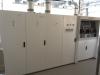
Picture 1 – CCS MOCVD installed and commissioned at the UMI-Georgia Tech-CNRS in Metz, France.
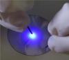
Picture 2 – A full 2-inch LED device wafer grown using the CCS MOCVD emitting blue light.
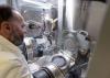
Picture 3 – ECE Professor Abdallah Ougazzaden loads the susceptor of MOCVD system.
Summary
The UMI-Georgia Tech-CNRS, an international research lab based in Metz, France at Georgia Tech-Lorraine (GTL), has successfully completed a process demonstration on the new Aixtron MOCVD system by growing a variety of III-nitrides and device structures, including Light Emitting Diodes and High Electron Mobility Transistors (HEMTS).
Status
- Workflow Status:Published
- Created By:Jackie Nemeth
- Created:09/14/2015
- Modified By:Fletcher Moore
- Modified:10/07/2016
Categories