news
Wafer bonding solution to epitaxial graphene – silicon integration
Primary tabs
Authors: Rui Dong, Zelei Guo, James Palmer, Yike Hu, Ming Ruan, John Hankinson, Jan Kunc, Swapan K Bhattacharya, Claire Berger, Walt A. de Heer
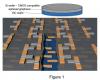
The development of graphene electronics requires the integration of graphene devices with Si-CMOS technology. Most strategies involve the transfer of graphene sheets onto silicon, with the inherent difficulties of clean transfer and subsequent graphene nano-patterning that degrades considerably the electronic mobility of nanopatterned graphene. Epitaxial graphene (EG) by contrast is grown on an essentially perfect crystalline (semi-insulating) surface, and graphene nanostructures with exceptional properties have been realized by a selective growth process on tailored SiC surface that requires no graphene patterning. However, the temperatures required in this structured growth process are too high for silicon technology. Here we demonstrate a new graphene to Si integration strategy, with a bonded and interconnected compact double-wafer structure. Using silicon-on-insulator technology (SOI) a thin monocrystalline silicon layer ready for CMOS processing is applied on top of epitaxial graphene on SiC. The parallel Si and graphene platforms are interconnected by metal vias. This method inspired by the industrial development of 3d hyper-integration stacking thin-film electronic devices preserves the advantages of epitaxial graphene and enables the full spectrum of CMOS processing.
Summary
The development of graphene electronics requires the integration of graphene devices with Si-CMOS technology. Most strategies involve the transfer of graphene sheets onto silicon, with the inherent difficulties of clean transfer and subsequent graphene nano-patterning that degrades considerably the electronic mobility of nanopatterned graphene.
Groups
Status
- Workflow Status:Published
- Created By:Gina Adams
- Created:11/15/2013
- Modified By:Fletcher Moore
- Modified:10/07/2016
Categories
Keywords