news
What is new in Packaging @ Georgia Tech? 5G Systems in 3D
Primary tabs
5G networks have been expected as a follow-on to 4G for a decade, with 100X higher wireless data rates and 100X lower latency than with current 4G networks. Unlike 4G, which was limited to mobile phones, 5G is expected to be used in pervasive applications and is expected to account for more than $400B, worldwide by 2022. These applications can be classified into three categories: a) enhanced mobile broadband with multi-Gbps data rates, b) massive internet of things for autonomous driving, smart-cities, wearables and smart-homes; and c) mission-critical services with low latency, high security, and reliability for automotive, healthcare and robotics.
5G modules scale bandwidth in two distinct domains by embedded or non-embedded 3D packaging: (1) in sub-6GHz bands with massive MIMO, requiring 5x or more component density than with 4G LTE, and (2) in mm-wave bands starting at 28GHz and 39GHz. The package challenges are many and include a new and unparalleled set of low-loss dielectric materials and ultra-precision processes. Unlike with 4G, antenna arrays need to be integrated in the 3D package with smaller sizes and ultra-low transmission losses, below 0.1 dB/mm, enabled by ultra-small, 2% process variations to meet stringent in-band loss and out-of-band rejection specifications. Heterogeneous integration in 3D ultra-thin packages is needed to achieve better component densities and performance than with the existing 2D organic laminate packages. The industry has pursued thick multilayer organic (MLO) packages with chips on one side and antenna arrays on the other side with through-vias such as by IBM, ASE and others who demonstrated such an antenna-in-package (AiP) phased-array system with transceiver dies flip-chip-attached to the backside of the package substrate. Organic packages, however, are limited by poor line-width control due to dimensional instability, requiring more layers with low process precision and high via transition losses, resulting in thicker packages. Fan-out wafer-level packaging is being developed for 5G modules to address these challenges with precision and low losses, antennas and through-via transition losses but at a high cost.
Georgia Tech proposes and develops ultra-thin laminated and large-panel 3D-glass packaging in two different architectures: with and without embedding, from sub-6GHz to mm-wave modules. Georgia Tech approach is a hybrid approach involving ultra-thin and ultra-low loss polymers and large ultra-thin glass, together achieving an unparalleled set of properties not possible with other packaging technologies, making Georgia Tech approach unique and superior. Glass, as a thin but high modulus core provides exceptional dimensional stability, with minimum warpage that is required to achieve the 2% process precision across the panel. Also, the glass panel is ultra-thin (<100 microns) and with an ultra-smooth surface finish, unlike laminate cores. Its TCE (thermal coefficient of expansion) can be matched perfectly to Si but can also be optimized for both chip- and board-level reliabilities simultaneously. The performance superiority, however, comes from ultra-low loss dielectrics on the glass surfaces and around copper through-vias. Such a hybrid approach achieves ultra-low loss of PTFE–like materials (polytetrafluoroethylene) while improving RDL circuit precision by up to 10X compared to multilayer organics. Through-package vias (TPVs) in glass can be scaled to 30-50 microns pitch and, even smaller in thinner glass substrates, compared to 300mm or larger pitch in organic laminates and molded embedded packages. The Georgia Tech approach is also superior in reducing the size of the modules as it enables double-side integration and assembly of active and thin-film passive components with the lowest loss, thus reducing the X-Y footprint of the modules by about half, and reducing the interconnect length between them to less than 100 microns. By scaling to 510 mm panel size manufacturing, the Georgia Tech 5G packaging can lower the cost compared to wafer-level packages. One example of laminated 5G glass package is illustrated in Fig. 1. Such a 3D structure has the following attributes:
- Lower via transition losses with smaller geometries
- Lower losses from chip to an antenna, enabled by shorter vertical and lateral interconnections
- Package-integrated antennas
- Thin-film low-pass and band-pass filters
- 3D package architecture with actives and passives on both sides, thus reducing the overall size.
These are briefly described below:
-
Low via transition losses with smaller geometries: Smaller vias that are enabled by thin glass show better performance such as lower insertion and return losses because of the impedance of the smaller vias matching perfectly with the transmission lines. Due to the better impedance match to the waveguides, their Voltage Wave Standing Ratio (VSWR) is nearly equal to one. This greatly reduces the signal bounce back to the source and hence a lower delay and greater bandwidth. Nearly the same via and capture pad sizes, which is only possible with the Georgia Tech’s laminated glass approach, results in significantly improved signal transmission performance by offering lower parasitic and reduced resonances at 5G frequencies. In addition, through-vias in a laminated glass does not show nonlinear effects, which greatly helps in suppressing the high-frequency noise harmonics. Georgia Tech has demonstrated small via formation, low-loss and ultra-short interconnections with 0.038 dB/microvia and 0.079 dB/through-substrate via at 5G frequencies. 22% bandwidth with 4.2 dBi gain with Yagi-Uda antennas on glass
-
Low interconnection losses: Ultra-thin buildup films with ultra-low dielectric loss enable ultra-low-loss signal transitions between components. As compared to thick transmission lines in laminates, thin transmission line structures in laminated glass substrates with insertion losses of 0.05 dB/mm have been demonstrated, as illustrated in Fig. 2. The superiority of laminated glass to form precision circuitry is also expected to further lower the losses. Interconnect losses in this hybrid glass approach, combined with the loss tangent of >0.005 of polymer dielectric, is shown to be superior to those with just low-loss LCP or other Teflon-like materials, with loss tangents <0.002. This is because of the other benefits of glass such as precision circuitry, smoothness of conductors and exceptional impedance match.
-
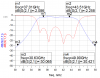
Package-integrated antennas with high gain: Laminated glass, in combination with low-loss polymer films, enables new opportunities for superior bandwidth and high antenna gain, and miniaturization of antenna arrays. Georgia Tech has recently demonstrated Yagi-Uda antennas and Horn antennas to achieve high gain and high bandwidth with excellent coverage. Single elements for both structures are designed to have >4 dBi with 20% bandwidth in 28 and 39 GHz bands. Such superior performance of Yagi-Uda antenna designs with thin laminated glass is shown in Fig.3.
-
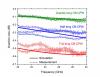
Thin-film low-pass and band-pass filters: The Georgia Tech’s approach enables high-quality distributed passive components such as filters and couplers with high-precision. The advanced RDL developed in the 5G project further enables ultra-miniaturized 5G packages in 3D. Using some of the most advanced RDL design rules, 5G distributed band-pass filters are designed with the size of about one-quarter wavelength in free space (λ0) corresponding to the cut-off or center frequency. The Georgia Tech laminated-glass approach enables low insertion loss in passband (~2 dB) along with >30 dB rejection in stopband, as illustrated with bandpass filters in Fig. 4, enabling new opportunities for broadband package designs.
-
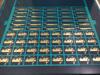
3D package for 5G with actives such as transceiver ICs, controllers, amplifiers and switches in ultra-thin 3D glass packages is being developed using two approaches: a) Chip-last with a double-sided assembly of actives, b) Chip-first with glass-panel embedding (GPE). Small-pitch through-vias in ultra-thin substrates, and large-area and high-throughput substrate processing tools and processes such as laser vias and double-side metallization techniques allow interconnecting the components on both sides with advanced panel processes to achieve lower cost. Large copper structures in 3D glass have also ben been demonstrated to eliminate the hotspots and reliability issues with embedded high-power dies. GT and its partners have recently demonstrated such 5G glass panels, as shown in Fig. 5. The precision impedance matching was shown to significantly lower the insertion loss.
The 5G project is in collaboration with several industry partners, including glass companies such as Corning Glass, Asahi Glass, and Schott Glass for supplying the ultra-thin glass panels; low-loss dielectric material suppliers such as Ajinomoto, Rogers, JSR, Panasonic; tool companies such as Ushio for precision lithography and Disco for planarization, ESI for high-precision microvia and through-via formation, Atotech for supplying the chemistry for advanced metallization processes; module companies such as Murata and Samtec, and end-users such as Qualcomm and Samsung.
About the Authors
Atom Watanabe is a Ph.D. student in Prof. Rao Tummala’s group, being mentored by Drs. Raj and Sundaram. His research focus is on EMI shielding and mm-wave module integration. atom@gatech.edu.
Muhammad Ali is a Ph.D. student in Prof. Rao Tummala group, being mentored by Drs. Raj and Sundaram. His research focus is on design, fabrication, and characterization of 5G and mm-wave passive components. ali_cmi@gatech.edu.
Prof. Manos Tentzeris is a Ken Byers Professor in the ECE Department, Georgia Tech. etentze@ece.gatech.edu.
Dr. Raj Pulugurtha is a Research Professor in Prof. Tummala’s group. pm86@mail.gatech.edu.
Dr. Venky Sundaram is a Research Professor in Prof. Tummala’s group and a Deputy Director of the Center. vs24@mail.gatech.edu.
Prof. Rao Tummala is the Joseph M. Pettit Chair Professor in ECE and MSE, and the Director of Georgia Tech’s 3D Systems Packaging Research Center (GT PRC). rao.tummala@ece.gatech.edu.
Media

Summary
Status
- Workflow Status:Published
- Created By:cheath6
- Created:03/30/2018
- Modified By:cheath6
- Modified:03/30/2018
Categories