news
What is New @ GT in Packaging? Glass Panel Fan-out
Primary tabs
Georgia Tech and its industry partners develop next generation of ultra-thin and ultra-high I/O density panel and wafer fan-out packaging to close the interconnect gap for digital applications, thickness or miniaturization gap for analog, power, RF and mm-wave applications, and power and thermal gap for high-power applications.
All packages are fan-out packages with the exception of chip-scale or wafer-level packages. These fan-out packages fall into two categories: chip-first, also called embedded, and chip-last. Both provide wiring or RDL to connect to ICs at fine or coarse pitch. In the chip-first approach, RDL is deposited directly onto ICs thus requiring no assembly; in contrast, in the chip-last process, two separate processes, one to form RDL with or without a substrate and second to assemble ICs to the wiring layers.
Fan-out wafer-level packages (FO-WLP), as extension of wafer-level packages, provide RDL wiring and I/Os beyond ICs on the surface of molding compounds. These packages, therefore, are no longer limited by I/Os and are thus poised to disrupt the entire semiconductor industry due to their benefits in performance, due to ultra-short interconnections, and wafer-based manufacturing infrastructure availability, compared to traditional flip-chip or wire bond packages. Two sets of applications are driving the need for fan-out packages: 1) analog applications that include RF, mm-wave such as Radar, and power for consumer electronics, using smaller and thinner devices to achieve thin packages with high component densities; and 2) digital applications to embed processors with larger ICs at higher I/O densities. The scope of FO-WLP technology is being proposed and developed in recent years to include multi-component SiP modules and integrated logic and 3D memory stacks to achieve high bandwidth.
But wafer fan out, as practiced today, has three major limitations: High cost, small Package size and low I/O density. Cost and package size limitations are due to small 300 mm wafers from which these fan-out packages are produced and low I/O density due to molding compound-driven challenges.
To address some of these concerns, panel-fanout Packaging (FO PLP) is beginning to emerge as a major new frontier. The economies of scale of panel-based processing may reduce FO-WLP cost by as much as 2-4x, depending on the package size, with the number of dies per package, the number of RDL layers and the panel size. FO PLP technologies can be broadly classified into two categories: 1) PWB infrastructure-based panel fan-out such as Imbera’s Integrated Module Board (IMB), AT&S’s Embedded Components Packaging (ECP), and ASE’s advanced – Embedded Assembly Solution Integration (a-EASI); Amkor and J-Devices Wide Strip Panel Fan-out Package (WFOP); and 2) LCD infrastructure-based panel fan-out that include PTI’s molded fan-out using 370mm x 470mm panels, and most recently by Samsung LSI, Samsung Display and SEMCO by repurposing idled Gen 3.25 (600mm x 720mm) and Gen 4 (730mm x 920mm) LCD lines.
Thev next generation of panel fan-out evolution must address three barriers:
- Interconnect gap for digital applications
- Thickness or miniaturization gap for analog, power, RF and mm-wave, and
- Thermal and power gap for high-power applications.
Georgia Tech and its 50 industry partners are developing next generation of panel fan-out in both chip-first and chip-last approaches to address these barriers, not only for computing and communications applications, but also for high-temperature and high-power automotive applications. In contrast to the wafer fan-out with molding compounds and laminate-based panel fan-outs, both can generally be referred to as organic-based, Georgia Tech’s approach is based on inorganic panel fan-out, either with glass as GFO or poly-silicon fan-out as PSFO.
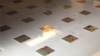
The Georgia Tech Glass Fan-out (GFO) approach addresses the interconnect gap with Si BEOL-like wiring, currently at 20 µm pitch. In addition, GFO provides lower interconnect loss, and higher board-level reliability even with large package sizes. The silicon-like dimensional stability of glass in large-panel manufacturing brings an unparalleled combination of ultra-high I/O density, ultra-high electrical performance, ultra-high reliability at low and high-temperature and low cost, not possible in molding compound-based or laminate-based fan-out technologies. With the low-loss of glass, being a factor of ~2-3x better than molding compounds, Georgia Tech’s GFO approach is ideal for RF and mm-wave modules. Unlike large high-density fan-out packages that require another package such as organic BGA package to connect to boards, GFO packages are designed to be directly SMT-attached to the board, enabled by the tailorability of the CTE of the glass panels and compliant interconnections. Lastly, the ultra-smooth surface and high dimensional stability of glass enables silicon-like RDL capability on large panels, for the first time, with less than 2µm critical dimensions (CD) for high density fan-out applications.
The GFO project is part of Georgia Tech’s industry consortium, supported by a number of industry partners, including Corning Glass, Asahi Glass, and Schott Glass that supply ultra-thin glass panels with cavities; Ushio that has placed a panel lithographic tool at Georgia Tech; Atotech that provides the plating chemistry for advanced metallization; and DISCO that has placed a low-cost planarization tool at Georgia Tech. End user applications for GFO in the Georgia Tech consortium include 5G, automotive camera and RADAR modules, low- and high-power modules, and logic-to-3D memory modules.
About the Authors
Tailong Shi is a PhD student under the advisement of Prof. Rao Tummala. His research focus is on Design and Demonstration of glass fan-out (GFO) packages for 77GHz automotive RADAR and Camera modules. tshi@gatech.edu.
Dr. Venky Sundaram is a Research Professor and the Associate Director of Industry Programs at Georgia Tech PRC. vs24@mail.gatech.edu.
Dr. Fuhan Liu is a Research Professor and an Assistant Program Manager for the GFO program. fuhan.liu@ece.gatech.edu.
Dr. Vanessa Smet is a Research Professor and the Program Manager for the Interconnections & Assembly (I&A) and High-power program. vanessa.smet@prc.gatech.edu.
Prof. Rao Tummala is the Joseph M. Pettit Chair Professor in ECE and MSE, and the Director of Georgia Tech’s 3D Systems Packaging Research Center (GT PRC). rao.tummala@ece.gatech.edu.

Groups
Status
- Workflow Status:Published
- Created By:Karen May
- Created:10/10/2016
- Modified By:Karen May
- Modified:10/10/2016
Categories