news
Seeing Moire in Graphene
Primary tabs
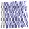
Researchers at the Georgia Institute of Technology and the National Institute of Standards and Technology (NIST) have demonstrated that atomic scale moiré patterns, an interference pattern that appears when two or more grids are overlaid slightly askew, can be used to measure how sheets of graphene are stacked and reveal areas of strain. The ability to determine the rotational orientation of graphene sheets and map strain is useful for understanding the electronic and transport properties of multiple layers of graphene, a one-atom thick form of carbon with potentially revolutionary semiconducting properties. The research appears in the journal, Physical Review B, in volume 81, issue 12.
In digital photography, moiré (pronounced mwar-ray) patterns occur because of errors in the rendering process, which causes grid patterns to look wavy or distorted. Materials scientists have been using microscopic moiré patterns to detect stresses such as wrinkles or bulges in a variety of materials.
Researchers created graphene on the surface of a silicon carbide substrate at the Georgia Institute of Technology by heating one side so that only carbon, in the form of multilayer sheets of graphene, was left. Using a custom-built scanning tunneling microscope at NIST, the researchers were able to peer through the topmost layers of graphene to the layers beneath. This process, which the group dubbed "atomic moiré interferometry," enabled them to image the patterns created by the stacked graphene layers, which in turn allowed the group to model how the hexagonal lattices of the individual graphene layers were stacked in relation to one another.
Unlike other materials that tend to stretch out when they cool, graphene bunches up like a wrinkled bed sheet. The researchers were able to map these stress fields by comparing the relative distortion of the hexagons of carbon atoms that comprise the individual graphene layers. Their technique is so sensitive that it is able to detect strains in the graphene layers causing as little as a 0.1 percent change in atom spacing.
“There’s an ideal atomic lattice spacing in graphene. Knowing the strain distribution can help us in our efforts to create graphene with good electronic properties,” said Phillip N. First, professor in the School of Physics at Georgia Tech. “So far, it looks as if multi-layered graphene has excellent conduction properties and may be useful for electronic applications.”
This collaboration between Georgia Tech and NIST is part of a series of experiments aimed at gaining a fundamental understanding of the properties of graphene. Other examples of the group's work can been seen at www.mrs.org/s_mrs/bin.asp?CID=8684&DID=320520&DOC=FILE.PDF and www.mrs.org/s_mrs/bin.asp?CID=26616&DID=320529&DOC=FILE.PDF.
Their article, "Structural analysis of multilayer graphene via atomic moiré interferometry" was selected as an Editor's Highlight in Physical Review B for the month of March, 2010.
Writers: Mark Esser and David Terraso
Summary
Researchers at the Georgia Institute of Technology and the National Institute of Standards and Technology have demonstrated that atomic scale moiré patterns, an interference pattern that appears when two or more grids are overlaid slightly askew, can be used to measure how sheets of graphene are stacked and reveal areas of strain.
Groups
Status
- Workflow Status:Published
- Created By:David Terraso
- Created:05/05/2010
- Modified By:Fletcher Moore
- Modified:10/07/2016
Categories